- 您现在的位置:买卖IC网 > Sheet目录512 > SI5975DC-T1-GE3 (Vishay Siliconix)MOSFET 2P-CH 12V 3.1A CHIPFET
Si5975DC
Vishay Siliconix
Dual P-Channel 12 V (D-S) MOSFET
PRODUCT SUMMARY
FEATURES
V DS (V)
- 12
R DS(on) ( Ω )
0.086 at V GS = - 4.5 V
0.127 at V GS = - 2.5 V
0.164 at V GS = - 1.8 V
I D (A)
- 4.1
- 3.4
- 3.0
? Halogen-free According to IEC 61249-2-21
Definition
? TrenchFET ? Power MOSFETs: 1.8 V Rated
? Compliant to RoHS Directive 2002/95/EC
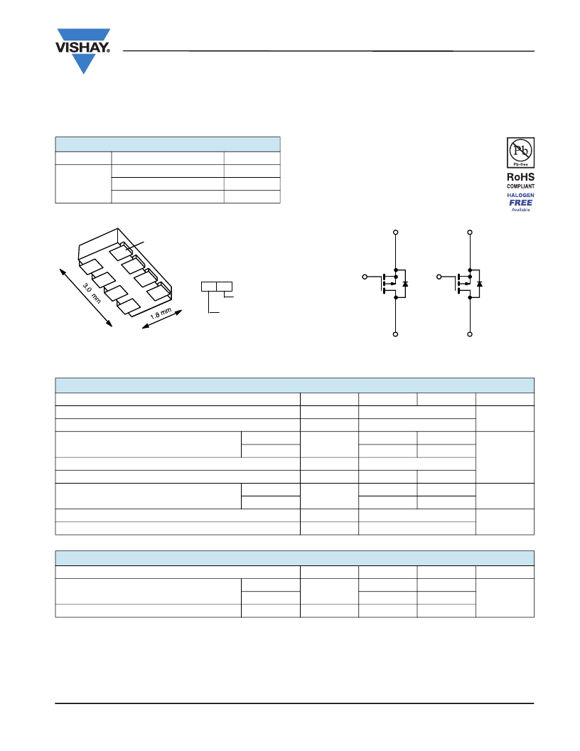
1206-8 ChipFET ?
S 1
1
S 1
S 2
D 1
G 1
D 1
S 2
Marking Code
G 1
G 2
DD XX
D 2
D 2
G 2
Lot Traceability
and Date Code
Part # Code
Bottom View
Ordering Information: Si5975DC-T1-E3 (Lead (Pb)-free)
Si5975DC-T1-GE3 (Lead (Pb)-free and Halogen-free)
D 1
P-Channel MOSFET
D 2
P-Channel MOSFET
ABSOLUTE MAXIMUM RATINGS T A = 25 °C, unless otherwise noted
Parameter
Drain-Source Voltage
Gate-Source Voltage
Symbol
V DS
V GS
5s
- 12
±8
Steady State
Unit
V
Continuous Drain Current (T J = 150 °C) a
Pulsed Drain Current
T A = 25 °C
T A = 85 °C
I D
I DM
- 4.1
- 3.0
- 10
- 3.1
- 2.2
A
Continuous Source Current (Diode Conduction) a
I S
- 1.8
- 0.9
Maximum Power Dissipation a
Operating Junction and Storage Temperature Range
Soldering Recommendations (Peak Temperature) b, c
T A = 25 °C
T A = 85 °C
P D
T J , T stg
2.1
1.1
- 55 to 150
260
1.1
0.6
W
°C
THERMAL RESISTANCE RATINGS
Parameter
Symbol
Typical
Maximum
Unit
Maximum Junction-to-Ambient a
Maximum Junction-to-Foot (Drain)
t ≤ 5s
Steady State
Steady State
R thJA
R thJF
50
90
30
60
110
40
°C/W
Notes:
a. Surface mounted on 1" x 1" FR4 board.
b. See reliability manual for profile. The ChipFET is a leadless package. The end of the lead terminal is exposed copper (not plated) as a result
of the singulation process in manufacturing. A solder fillet at the exposed copper tip cannot be guaranteed and is not required to ensure
adequate bottom side solder interconnection.
c. Rework conditions: manual soldering with a soldering iron is not recommended for leadless components.
Document Number: 71320
S10-0936-Rev. C, 19-Apr-10
www.vishay.com
1
发布紧急采购,3分钟左右您将得到回复。
相关PDF资料
SI5980DU-T1-GE3
MOSFET N-CH 100V PPAK CHIPFET
SI6404DQ-T1-GE3
MOSFET N-CH 30V 8.6A 8TSSOP
SI6413DQ-T1-E3
MOSFET P-CH 20V 7.2A 8TSSOP
SI6423DQ-T1-GE3
MOSFET P-CH 12V 8.2A 8-TSSOP
SI6466ADQ-T1-GE3
MOSFET N-CH 20V 6.8A 8TSSOP
SI6467BDQ-T1-GE3
MOSFET P-CH 12V 6.8A 8TSSOP
SI6924AEDQ-T1-GE3
MOSFET N-CH 28V ESD 8-TSSOP
SI6926ADQ-T1-GE3
MOSFET DL N-CH 20V 4.5A 8-TSSOP
相关代理商/技术参数
SI5980DU-T1-GE3
功能描述:MOSFET 100V 2.5A 7.8W .567Ohms @ 10V RoHS:否 制造商:STMicroelectronics 晶体管极性:N-Channel 汲极/源极击穿电压:650 V 闸/源击穿电压:25 V 漏极连续电流:130 A 电阻汲极/源极 RDS(导通):0.014 Ohms 配置:Single 最大工作温度: 安装风格:Through Hole 封装 / 箱体:Max247 封装:Tube
SI5997DU-T1-GE3
功能描述:MOSFET 30V 6A 10.4W 54mOhms @ 10V RoHS:否 制造商:STMicroelectronics 晶体管极性:N-Channel 汲极/源极击穿电压:650 V 闸/源击穿电压:25 V 漏极连续电流:130 A 电阻汲极/源极 RDS(导通):0.014 Ohms 配置:Single 最大工作温度: 安装风格:Through Hole 封装 / 箱体:Max247 封装:Tube
SI5999EDU-T1-GE3
功能描述:MOSFET 20V 6A DUAL P-CH MOSFET RoHS:否 制造商:STMicroelectronics 晶体管极性:N-Channel 汲极/源极击穿电压:650 V 闸/源击穿电压:25 V 漏极连续电流:130 A 电阻汲极/源极 RDS(导通):0.014 Ohms 配置:Single 最大工作温度: 安装风格:Through Hole 封装 / 箱体:Max247 封装:Tube
SI-5L1.880G
制造商:HITACHIMETAL 功能描述:
Si5XX5X7-EVB
功能描述:时钟和定时器开发工具 XO / VCXO Device Evaluation Board RoHS:否 制造商:Texas Instruments 产品:Evaluation Modules 类型:Clock Conditioners 工具用于评估:LMK04100B 频率:122.8 MHz 工作电源电压:3.3 V
Si5XX-EVB
功能描述:时钟和定时器开发工具 Si5XX EVAL Board RoHS:否 制造商:Texas Instruments 产品:Evaluation Modules 类型:Clock Conditioners 工具用于评估:LMK04100B 频率:122.8 MHz 工作电源电压:3.3 V
Si5xx-PROG-EVB
功能描述:时钟和定时器开发工具 I2C Programmable Evaluation Kit RoHS:否 制造商:Texas Instruments 产品:Evaluation Modules 类型:Clock Conditioners 工具用于评估:LMK04100B 频率:122.8 MHz 工作电源电压:3.3 V
SI5XXUC-EVB
功能描述:XO & VCXO UNIVERSAL EVAL BOARD 制造商:silicon labs 系列:- 零件状态:在售 主要用途:计时,时钟振荡器 嵌入式:- 使用的 IC/零件:Si5xxUC 主要属性:- 辅助属性:- 所含物品:板 标准包装:1
